


Your phone, your car, the UPI machine at the corner shop and the hospital scanner all depend on tiny chips. Building a chip factory makes headlines. But factories are not enough if there are no trained people to design what goes inside them. Karnataka is trying to fix that with a programme called K-VLSI.
What happened?
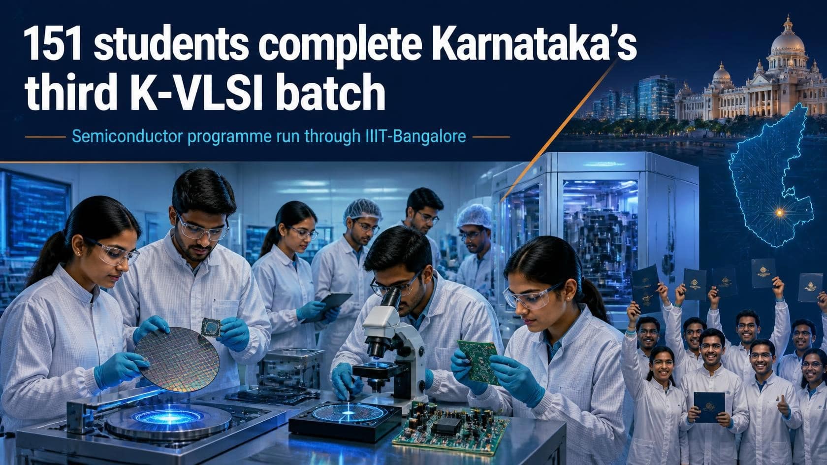
The K-VLSI Post Graduate Diploma Programme, a semiconductor skilling initiative of the Government of Karnataka, completed its third batch. The graduation ceremony was held in Bengaluru on 2 October 2026, and 151 students graduated. IT-BT Minister Priyank Kharge shared the news on LinkedIn.
What is VLSI, in simple words?
VLSI stands for Very Large Scale Integration. It means packing millions or billions of tiny electronic switches onto one small chip. Engineers who design and test these chips are in short supply, and that gap is what K-VLSI tries to close.
How does the programme work?
The programme is run by the Centre of Excellence MINRO at IIIT-Bangalore for the state’s IT-BT Department, together with the Karnataka Digital Economy Mission (KDEM) and the India Electronics and Semiconductor Association (IESA). It combines classroom learning with practical lab training, design and verification projects, mentorship from semiconductor professionals and placement support.
Verification means testing a chip design on a computer to find mistakes before the chip is made. Errors found late are very costly to fix, so this skill is in demand.
It has also grown quickly. The first batch had 70 students, the second 144 and the third 151. The second batch was chosen from more than 3,000 applicants from over 40 towns, and its students came from over 60 engineering colleges. They did the diploma alongside their final engineering semester, so they were ready to work as soon as they graduated.
Do students actually get jobs?
According to the minister’s post, the first batch recorded close to 100% placement and the second about 90%. Graduates have joined companies such as BEL, IBM, Siemens, Samsung, Bosch, Tata Electronics, Foxconn and NXP. These figures were shared by the minister and have not been independently checked, so treat them as reported claims. The programme’s own page promises “placement assistance”, which is not a guarantee of a job.
How can students join?
Here is what the official programme page said for the first batch. Later batches may differ, so check the latest notice.
- Where to look: The KDEM programme page at karnatakadigital.in/k-vlsi has the details and a registration form. IIIT-Bangalore’s website is iiitb.ac.in.
- Who can apply: Engineers from Electronics, ECE, Computer Science, IT and related branches, who studied at a recognised college in Karnataka or have Karnataka domicile. The second batch took students who had finished their 7th semester.
- How students are selected: The first batch was shortlisted by engineering marks, then an online written test with the camera on (40 minutes, covering aptitude and digital design basics), then an interview on engineering fundamentals.
- Where the classes are: The first batch started at the IIIT-Bangalore campus in Electronics City, Bengaluru. Students from other cities arranged their own accommodation.
- How long it lasts: The first batch ran for 6 months in hybrid mode, with the first two months attended in person. A course page for the third batch mentions 26 weeks.
- What it costs: The programme is valued at over ₹2.5 lakh, and a selected student in the first batch paid ₹15,000 (the page states this both as plus GST and as inclusive of GST). The rest is covered by the government and its partners.
- Who to contact: KDEM, KEONICS, 27th Main Road, 1st Sector, HSR Layout, Bengaluru 560102. The “Contact Us” page on karnatakadigital.in lists current phone and email details.
At the time of writing, no notice for a fourth batch had been published that I could find. Students should watch the KDEM website and LinkedIn page for dates.
Why does this matter?
- For students. A graduate from a small town gets a route into a high-skill field without leaving Karnataka.
- For companies. Chip makers say a lack of trained designers slows them down. A steady supply of graduates makes the state more attractive.
- For the state and the country. Karnataka wants to grow its semiconductor industry, and India wants to make more of its own chips. Factories need designers, and designers need training.
What to watch
- The numbers are small. 151 graduates a year is a good start, but the industry will need many thousands.
- Placement quality. Watch the roles, salaries and how many graduates stay in chip design.
- Fit with industry. The programme works only if what is taught keeps matching what employers need.
- Reach. The real test is whether students from smaller colleges and towns keep getting in.
The bottom line
A semiconductor industry is built from factories, money and people. Karnataka’s K-VLSI programme is working on the people part. If the placement claims hold up as the batches grow, it could become a model for other states.
Sources: India Education Diary, CityAir News, IIIT-Bangalore, TimesTech, the Karnataka Digital Economy Mission and Priyank Kharge’s LinkedIn post, 2023 to October 2026.